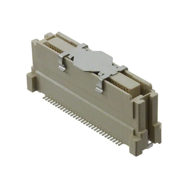
It uses a center strip contact arrangement across two rows on a 0.025" (0.64 mm) pitch, with gold-plated contacts at 10.0 µin thickness. It is intended for dense signal routing where the board stack height needs to be chosen from a range of 11 mm, 12 mm, 13 mm, 14 mm, 15 mm, or 16 mm — the six mated stacking heights let the board layout engineer tune the z-height budget without changing the footprint.
The 0.025" (0.64 mm) pitch is the tightest selection parameter — it sets the routing density and the footprint class for the PCB layout engineer. The six mated stacking heights (11 mm, 12 mm, 13 mm, 14 mm, 15 mm, 16 mm) are the primary selection axis for board-to-board spacing: the buyer matches their z-height budget by picking the height that fits between the two PCBs.