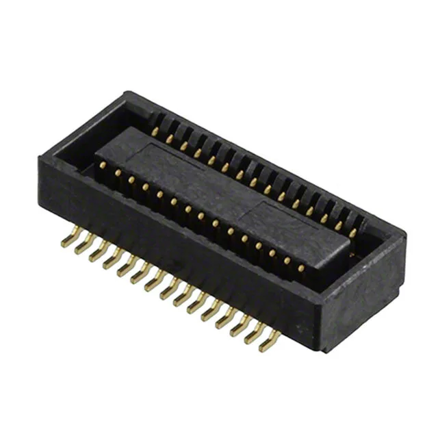
Board-Stacking Fit at 0.50mm Pitch
The 0.020" (0.50mm) pitch packs 30 circuits into a dual-row layout — each row carries 15 contacts, with center strip contacts between the rows that provide a natural ground reference for differential signal pairs. The 0.079" (2.00mm) height above board and 2.5mm mated stacking height define the z-axis clearance between the two PCBs; that 2.5mm gap is the dimension you design the enclosure standoffs around.
The gold-on-gold interface keeps contact resistance stable through the first several mates, which matters for signal integrity in a high-density differential pair layout.
Surface-Mount Assembly and Packaging
Surface-mount termination suits reflow soldering on standard SMT lines. The 0.50mm pitch means the PCB footprint needs tight solder paste registration — the pad layout in the product drawing is the one to follow, not a generic 0.50mm pattern.