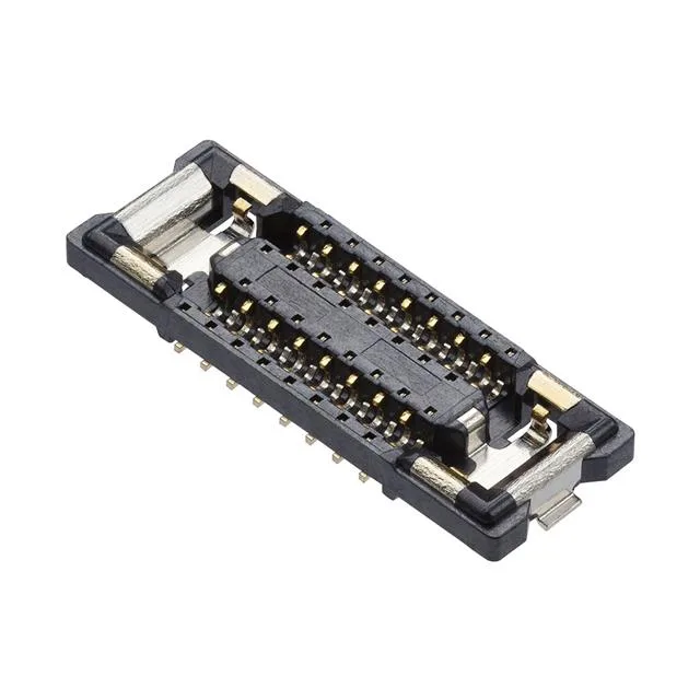
Board-Stacking Fit: 0.35mm Pitch and 0.6mm Gap
Its defining dimension is the 0.014" (0.35mm) pitch — that 0.35mm centre-to-centre spacing on the contacts drives the board layout: trace-and-space rules tighten, and via escape between pads requires micro-via or HDI techniques. The mated stack height of 0.6mm means the two PCBs sit less than a millimetre apart, typical for ultra-thin handheld or module-on-motherboard assemblies where every tenth of a millimetre of z-height matters.
Termination and Retention on the Board
At 0.35mm pitch, the SMT pads are small and the connector's own mass is low, but the solder tabs give the reflow joint extra shear resistance — useful when the mated board stack sees thermal cycling or mechanical shock. The gold contact finish (3.94µin / 0.100µm) is a flash plating; it protects the mating surface during the few insertion cycles a mezzanine connector typically sees in its lifetime, but it is not specced for repeated field disconnect.