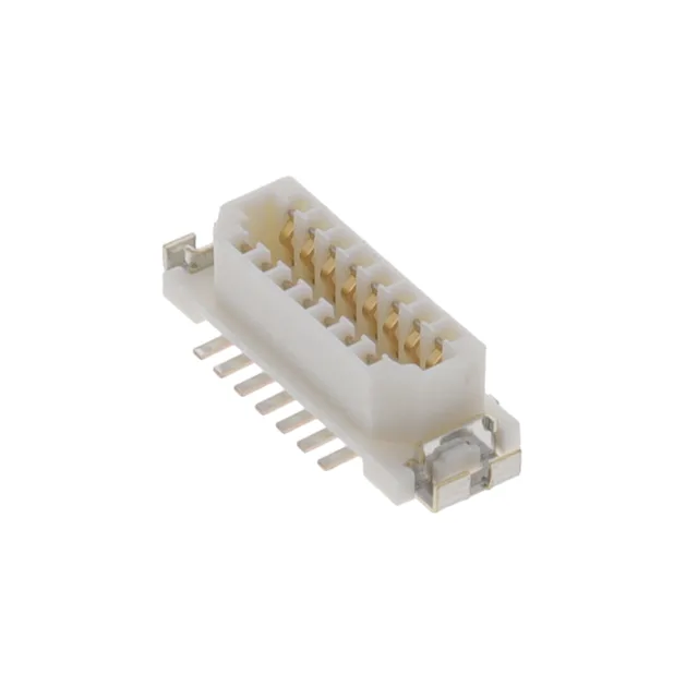
This connector is used in compact electronic assemblies where two PCBs need to be stacked parallel with a tight z-height budget — think handheld devices, portable instrumentation, or internal module interconnects. The 1.00mm pitch and 15 positions suit signal-density applications where a full 2.54mm pitch header would waste board area.
Position count and pitch — the footprint fit
The 15 positions at 0.039" (1.00mm) pitch define the PCB footprint. This is a dual-row layout, so the connector occupies 7.5 positions per row, giving a board edge footprint roughly 7.5mm wide plus the outer shroud. The 1.00mm pitch is tight enough that trace routing between pads requires a fine-line PCB capability, but it is standard for modern portable electronics. Tin is suitable for fewer mating cycles and benign environments; the gold-flash (69) variant is the better choice for corrosive atmospheres or applications requiring more than a few dozen mate-unmate cycles.
Mated stacking height — the z-height constraint
The mated stacking height is 4.3mm. This is the distance between the two PCBs when the receptacle is mated with its matching DF9 series header. It is a fixed, non-adjustable dimension — the board-to-board gap is determined by the connector pair, not by any spacer.