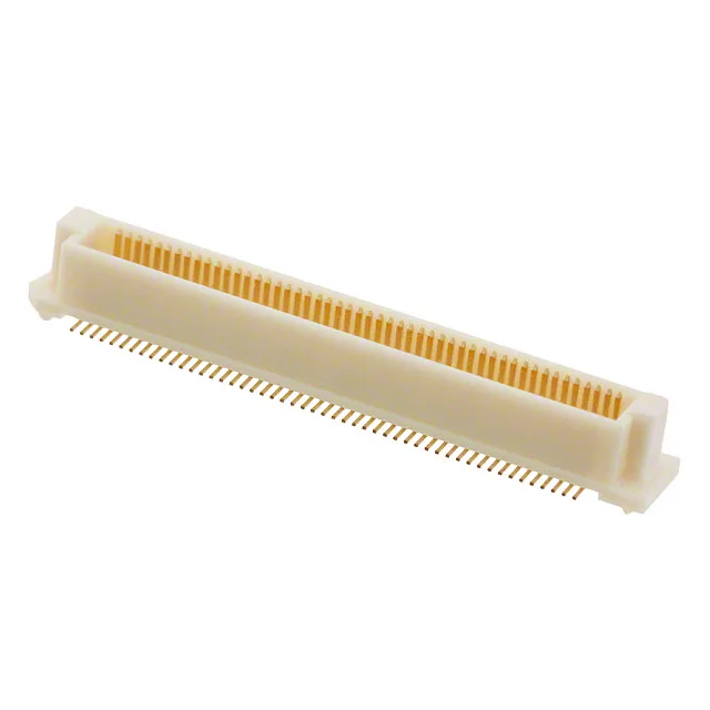
100-position mezzanine header at 0.60mm pitch — Hirose FX8C-100P-SV2(91)
The Hirose FX8C-100P-SV2(91) is a 100-position header from the FunctionMax™ FX8C series, designed for dense board-to-board mezzanine stacking.
Stack height options — 7mm and 12mm mated pairs
This header is rated for mated stacking heights of 7mm and 12mm, meaning the board-to-board gap after mating the receptacle is set by the pair's combined height. The 6.45mm standoff on this header leaves room for the mating receptacle's profile to hit either target. That dual-height capability gives the layout engineer flexibility: the same header can serve a low-profile stack (7mm) or a taller one (12mm) by swapping only the receptacle half, without requalifying the footprint.
Gold-plated contacts in a two-row array
The two-row arrangement keeps the connector body narrow, which helps route traces out of the inner row on the PCB without excessive via fanout.
Board guide and SMT mounting for automated assembly
Surface-mount termination suits reflow soldering on standard PCB processes; the tube packaging (not tape-and-reel on this suffix) means it feeds through tube feeders or can be hand-placed for prototype runs.
Height variants in the same 100-position footprint
The FX8C series offers three height variants at 100 positions, all sharing the same 0.60mm pitch and gold-plated two-row layout. The FX8C-100P-SV2(91) at 0.254" (6.45mm) sits between the shorter FX8C-100P-SV(91) at 0.175" (4.45mm) and the FX8C-100P-SV1(91) at 0.214" (5.45mm). The choice between them is driven purely by the mated stack height target — 7mm or 12mm for the SV2, versus shorter stack heights for the SV and SV1. All three use the same PCB footprint, so swapping heights mid-design requires no board layout change.
No official successor or replacement has been issued — this is the current production version.
The outer shroud contacts on the header engage with the receptacle's inner contact beams, providing a shrouded interface that resists dust ingress and prevents stubbing during blind mating. Typical deployment is in parallel PCB stacks inside telecom switches, data routers, or industrial controllers where signal density and board spacing are both constrained.