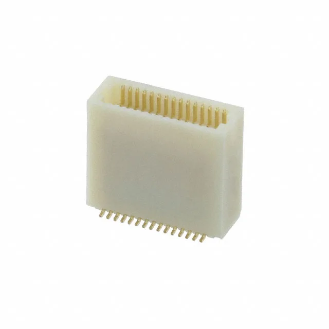
30P9.0-JMCS-G-B-TF — JST product photo

JST 30P9.0-JMCS-G-B-TF JMC Series Plug, 30 Pos, 0.50mm Pitch

MPN30P9.0-JMCS-G-B-TF
Obsolete

JST JMC series plug, outer shroud contacts, 30 positions, 2 rows, 0.020" (0.50mm) pitch, 9mm mated stack height, gold contact finish, surface mount, board guide.

$1.4200Ref. price · indicative, final on quote
StockContact for availability
MOQ1 pcs
  • New & original stockTraceable channels only — no mixed lots, no re-taped reels.
  • Factory packaging where availableSealed reels, trays and bags; cut quantities always stated on the quote.
  • Photo-verified countsEvery line counted and photographed before the box closes.
  • PayPal buyer protectionPay by T/T, PayPal or Payoneer — card payments covered end to end.

Specifications

30P9.0-JMCS-G-B-TF Technical Specifications
ParameterValue
SeriesJMC
Mounting typeSurface Mount
Connector typePlug, Outer Shroud Contacts
Mated stacking heights9mm
Pitch0.020\" (0.50mm)
PackageCut Tape (CT)
FeaturesBoard Guide
Contact finishGold
Rows2
Positions30

Product details

JST 30P9.0-JMCS-G-B-TF — JMC Series Board-to-Board Plug

The mated stack height is 9mm, giving a fixed z-height budget for the enclosure. Gold contact finish handles the repeated mating cycles typical of production test or field-service connections. A built-in board guide helps align the plug during assembly, taking shear off the fine-pitch contacts.

Frequently asked questions

Where can I buy 30P9.0-JMCS-G-B-TF?

30P9.0-JMCS-G-B-TF is obsolete and no longer in factory production.

What is the direct replacement for 30P9.0-JMCS-G-B-TF?

JST has not published an official successor order code for 30P9.0-JMCS-G-B-TF. Any replacement must be a parametric match — same 0.50mm pitch, 30 positions, 9mm stack height, gold-plated outer shroud contacts, SMT — verified against the original PCB footprint.

What is the stack height and pitch of 30P9.0-JMCS-G-B-TF?

The mated stack height is 9mm, and the contact pitch is 0.020" (0.50mm). These two dimensions define the board-to-board clearance and the PCB routing density.