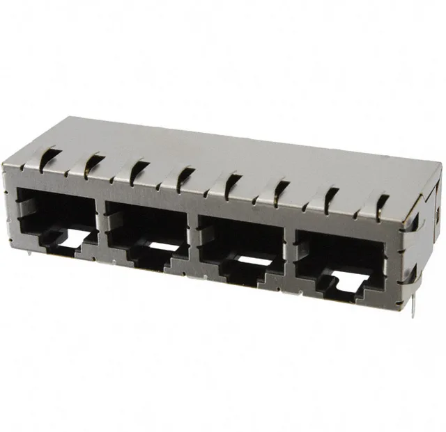
It is shielded with an integrated EMI finger and oriented tab-down. This is the 4-port member of the 6339167 base series, designed for a single PCB footprint that replaces four discrete jacks — saving placement cost and board real estate on Ethernet switch, router, industrial gateway, and PoE injector designs. The Cat5 rating means it supports 100 MHz signaling, adequate for 100BASE-TX and 1000BASE-T applications.
Shielded vs unshielded — the EMI finger makes the difference
The 6339167-3 carries a shielded shell with an EMI finger — a spring contact that grounds the shell to the panel or chassis ground plane. An unshielded RJ45 jack relies entirely on the twisted-pair cable for common-mode rejection; once the cable shield terminates at the plug, the 6339167-3's EMI finger bleeds that shield current to chassis before it reaches the PHY transformer. For equipment that must pass FCC Part 15 radiated emissions or EN 55032, this jack saves adding a separate grounding clip or ferrite. The tab-down orientation means the latch on the mating RJ45 plug faces the PCB — check your panel cutout and plug cable exit direction; a tab-up jack would flip the cable strain relief the other way.
Gold contacts rated for field reconnect duty
The tin-plated solder tails are compatible with standard lead-free wave or hand-solder processes. The housing is PCT/polyester, a high-temperature thermoplastic that survives lead-free reflow profiles without distortion.
Board layout notes for the 4-port ganged footprint
The right-angle through-hole termination and board guide feature mean the jack self-aligns during insertion — the board guide posts engage the PCB alignment holes before the solder tails enter their plated through-holes, preventing bent pins. The 4-port ganged body occupies roughly the width of four standard single-port jacks but with a single pick-and-place cycle. Tray packaging (not tape-and-reel) means the part feeds from a tray or tube feeder on the placement line — confirm your feeder setup handles tray components before committing the BOM. The EMI finger extends beyond the housing body; the keep-out zone on the PCB must allow clearance for the finger to contact the chassis or ground pad without shorting adjacent traces.