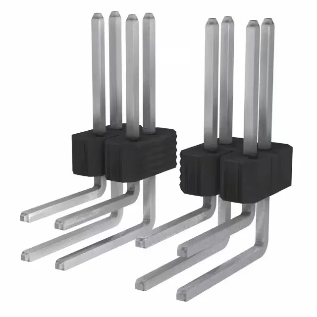
It uses a 0.100" (2.54 mm) pitch — the standard grid for legacy through-hole layouts and prototyping — and a right-angle through-hole termination that places the pin array parallel to the PCB, suited for edge-card or mezzanine stacking where vertical clearance is tight. The tin-on-tin interface is cost-effective for high-volume builds with limited mating cycles — the 100.0 µin (2.54 µm) plating thickness on the mating side provides adequate wear for repeated board-level connections in production or field service.
Board Layout and Fit
The 0.100" (2.54 mm) pitch and 0.100" row spacing define a 58-pin footprint that spans 29 positions per row. The mating pin length is 0.318" (8.08 mm), with a 0.230" (5.84 mm) solder tail — the post length is sized for standard 0.062" to 0.093" thick PCBs through a plated through-hole. Insulation height above the board is 0.190" (4.83 mm), leaving clearance for components under the header body.