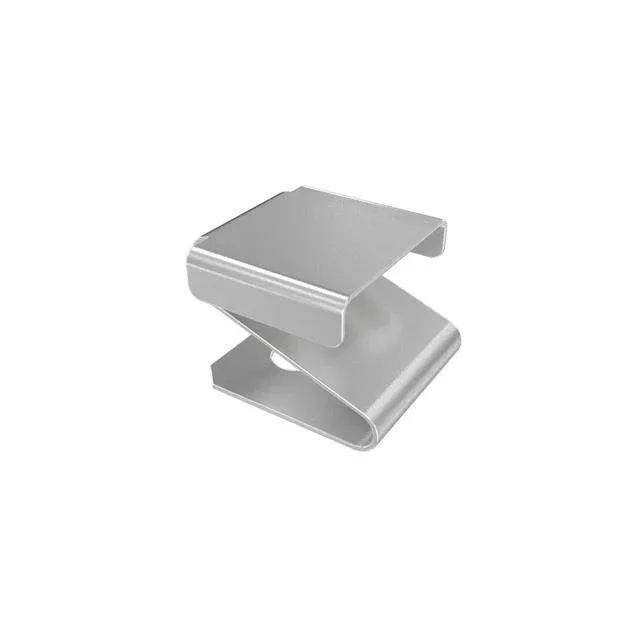
3.3 mm compressed height — the z-height that drives the board stack
The Z01B-4G7L1-11000-E000: The 3.3 mm compressed height is the dimension that decides the clearance between the board and the mating surface — a battery contact, a shield can, or another PCB. At that height the spring force keeps the contact pressed against the pad without bottoming out. Single-contact, single-row layout means one device per BOM line. If your design needs multiple spring points, you place one instance per contact position.
Stainless steel spring with gold flash — mechanical cycle life vs contact resistance
The gold flash on the contact face keeps the mating resistance low against a gold-plated pad. Flash gold is a thin deposit — adequate for intermittent signal contact where the connector isn't cycled hundreds of times. If the application needs repeated mating (test points, battery swap), the sibling Z01U-4G7L1-11000-E000 carries 8.00 µin gold for longer wear.
Surface-mount termination — no through-holes, no backside routing penalty
SMT pads sit on the top copper layer — the board area below the contact is free for traces or a ground plane. The non-gendered compression contact mates against a flat pad on the opposing surface, so no mating half is needed beyond the landing pad.