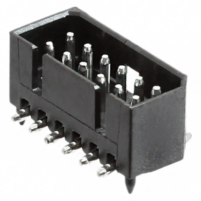
Board Fit and Signal Routing at 1.25 mm Pitch
The 0.049-inch pitch sets the PCB footprint — tight enough for dense signal routing on a two-layer board, but with enough clearance for a single via between pads on the inner rows. Surface-mount solder termination means the connector reflows with the board in a single pass. The PPS (polyphenylene sulfide) housing handles the reflow profile without warping, and the UL94 V-0 rating keeps it compliant for equipment inside an enclosure.