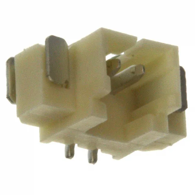
Board footprint and routing at 1.25 mm pitch
At 1.25 mm, the board footprint is compact enough for dense automotive or industrial control PCBs, but the narrow pitch limits per-contact current to 1 A and demands careful trace routing between pads.
Shroud and solder retention for assembly reliability
Current and voltage rating – signal-level duty
The tin-plated mating surface with 150.0 µin thickness provides adequate corrosion resistance for moderate-cycle applications, but the 1 A limit means it is not suited for power distribution.